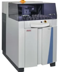
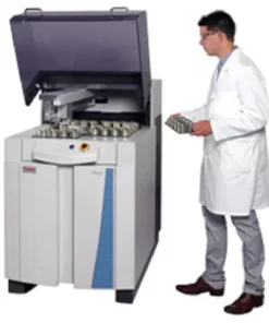
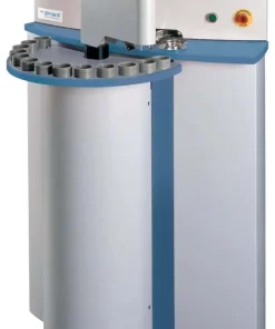
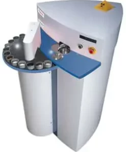
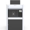
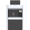
Talos F200i Transmission Electron Microscope
The Thermo Scientific Talos F200i (S)TEM is a 20-200 kV field emission (scanning) transmission electron microscope uniquely designed for performance and productivity across a wide range of Materials Science samples and applications. Its standard X-Twin pole piece gap—giving the highest flexibility in applications—combined with a reproducibly performing electron column opens opportunities for high-resolution 2D and 3D characterization, in situ dynamic observations, and diffraction applications.
Talos F200i Transmission Electron Microscope advantages
Designed for multi-user and multi-discipline environments, the Talos F200i (S)TEM is also ideal for novice users. It is equipped with the Thermo Scientific Velox user interface, which is immediately familiar since it is shared across all Thermo Scientific TEM platforms. All TEM daily tunings have been automated to provide the best and most reproducible setup. The Align Genie automation software eases the learning curve for novice operators, reduces tensions in a multi-user environment, and improves time-to-data for the experienced operator. A side-entry retractable Energy Dispersive X-ray Spectroscopy (EDS) detector can be added to the configuration to enable chemical analysis.
Available with a wide range of high-resolution field emissions guns (FEG)
Choose S-FEG, high-brightness X-FEG, or ultra-high-brightness Cold Field Emission Gun (X-CFEG). X-CFEG combines the best (S)TEM imaging with the best energy resolution.
Available with Dual EDS technology
Choose the best EDS detector for your needs, ranging from a single 30 mm² detector to dual 100 mm² detectors for high throughput (or low-dose) analytics.
High-quality STEM/TEM images and accurate EDS
Acquire high-quality TEM or STEM images with the innovative and intuitive Velox Software user interface in very a simple way. Unique EDS absorption correction in Velox Software enables the most accurate quantification.
Best all-round in situ capabilities
Add tomography or in situ sample holders. Fast cameras, smart software, and our wide X-TWIN objective lens gap enable 3D imaging and in situdata acquisition with minimal compromise to resolution and analytical capabilities.
Increased productivity
Ultra-stable column and remote operation with the SmartCam Camera and constant-power objective lenses for swift mode and high-voltage (HT) switches. Fast and easy switching for multi-user environments.
Most repeatable data
All daily TEM tunings, such as focus, eucentric height, beam shift, condenser aperture, beam tilt pivot points and rotation center are automated, ensuring you always start from optimum imaging conditions. Experiments can be repeated reproducibly, allowing more focus on research instead of the tool.
Large field-of-view imaging at high speed
The 4k × 4k Ceta CMOS camera with its large field of view enables live digital zooming with high sensitivity and high speed over the entire high-tension range.
Compact design
Smaller footprint and dimensions facilitate accommodating this tool in more challenging spaces while reducing infrastructure and support costs.
Process control using electron microscopy
Modern industry demands high throughput with superior quality, a balance that is maintained through robust process control. SEM and TEM tools with dedicated automation software provide rapid, multi-scale information for process monitoring and improvement.
Quality control and failure analysis
Quality control and assurance are essential in modern industry. We offer a range of EM and spectroscopy tools for multi-scale and multi-modal analysis of defects, allowing you to make reliable and informed decisions for process control and improvement.
Fundamental Materials Research
Novel materials are investigated at increasingly smaller scales for maximum control of their physical and chemical properties. Electron microscopy provides researchers with key insight into a wide variety of material characteristics at the micro- to nano-scale
Energy Dispersive Spectroscopy
Energy dispersive spectroscopy (EDS) collects detailed elemental information along with electron microscopy images, providing critical compositional context for EM observations. With EDS, chemical composition can be determined from quick, holistic surface scans down to individual atoms.
3D EDS Tomography
Modern materials research is increasingly reliant on nanoscale analysis in three dimensions. 3D characterization, including
Atomic-Scale EDS
Atomic-resolution EDS provides unparalleled chemical context for materials analysis by differentiating the elemental identity of individual atoms. When combined with high-resolution TEM, it is possible to observe the precise organization of atoms in a sample.
EDS Elemental Analysis
Thermo Scientific Phenom Elemental Mapping Software provides fast and reliable information on the distribution of chemical elements within a sample.
Electron Energy Loss Spectroscopy (EELS)
Materials science research benefits from high-resolution EELS for a wide range of analytical applications. This includes high-throughput, high signal-to-noise-ratio elemental mapping, as well as probing of oxidation states and surface phonons.
In Situ experimentation
Direct, real-time observation of microstructural changes with electron microscopy is necessary to understand the underlying principles of dynamic processes such as recrystallization, grain growth, and phase transformation during heating, cooling, and wetting.
Particle analysis
Particle analysis plays a vital role in nanomaterials research and quality control. The nanometer-scale resolution and superior imaging of electron microscopy can be combined with specialized software for rapid characterization of powders and particles.
Multi-scale analysis
Novel materials must be analyzed at ever higher resolution while retaining the larger context of the sample. Multi-scale analysis allows for the correlation of various imaging tools and modalities such as X-ray microCT, DualBeam, Laser PFIB, SEM and TEM.
Automated Particle Workflow
The Automated NanoParticle Workflow (APW) is a transmission electron microscope workflow for nanoparticle analysis, offering large area, high resolution imaging and data acquisition at the nanoscale, with on-the-fly processing.


")


 VI
VI