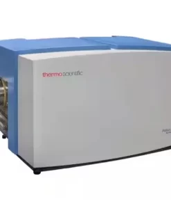
Talos F200S G2 Transmission Electron Microscope
The Thermo Scientific Talos F200S (S)TEM is a (scanning) transmission electron microscope that combines outstanding high-resolution STEM and TEM imaging with industry-leading energy dispersive X-ray spectroscopy (EDS). The Talos F200S (S)TEM features great versatility and high through in STEM imaging and allows for precise EDS analysis and high-resolution TEM (HRTEM) for dynamic microscopy.
Talos F200S G2 Transmission Electron Microscope advantages
The Thermo Scientific Talos F200S 200kV (S)TEM combines fast, multichannel, high-resolution (S)TEM imaging and precise compositional analysis to enable dynamic microscopy applications. With innovative features designed to increase throughput, precision, and ease of use, the Talos (S)TEM is ideal for advanced research and analysis across academic, government, and industrial research environments.
Intuitive software
Features Thermo Scientific Velox Software for fast and easy acquisition and analysis of multimodal data.
Precise chemical composition data
Rapid, precise, quantitative EDS analysis using two in-column Thermo Scientific SDD Super-X Detectors with unique cleanliness, revealing nanoscale details.
Better image data
High-throughput (S)TEM imaging with simultaneous, multiple signal detection delivers better contrast for high quality images.
Upgrade
Can be field upgraded to the Thermo Scientific Talos F200X (S)TEM.
Increased stability
Reduced environmental sensitivity thanks to the instrument enclosure, which moderates the impact of air pressure waves, air flows, and fine temperature variations in the TEM room.
Space for more
Add application-specific in situ sample holders for dynamic experiments.
Process control using electron microscopy
Modern industry demands high throughput with superior quality, a balance that is maintained through robust process control. SEM and TEM tools with dedicated automation software provide rapid, multi-scale information for process monitoring and improvement.
Quality control and failure analysis
Quality control and assurance are essential in modern industry. We offer a range of EM and spectroscopy tools for multi-scale and multi-modal analysis of defects, allowing you to make reliable and informed decisions for process control and improvement.
Fundamental Materials Research
Novel materials are investigated at increasingly smaller scales for maximum control of their physical and chemical properties. Electron microscopy provides researchers with key insight into a wide variety of material characteristics at the micro- to nano-scale
Energy Dispersive Spectroscopy
Energy dispersive spectroscopy (EDS) collects detailed elemental information along with electron microscopy images, providing critical compositional context for EM observations. With EDS, chemical composition can be determined from quick, holistic surface scans down to individual atoms.
3D EDS Tomography
Modern materials research is increasingly reliant on nanoscale analysis in three dimensions. 3D characterization, including compositional data for full chemical and structural context, is possible with 3D EM and energy dispersive X-ray spectroscopy.
EDS Elemental Analysis
Thermo Scientific Phenom Elemental Mapping Software provides fast and reliable information on the distribution of chemical elements within a sample.
Atomic-Scale EDS
Atomic-resolution EDS provides unparalleled chemical context for materials analysis by differentiating the elemental identity of individual atoms. When combined with high-resolution TEM, it is possible to observe the precise organization of atoms in a sample.
Electron Energy Loss Spectroscopy (EELS)
Materials science research benefits from high-resolution EELS for a wide range of analytical applications. This includes high-throughput, high signal-to-noise-ratio elemental mapping, as well as probing of oxidation states and surface phonons.
In Situ experimentation
Direct, real-time observation of microstructural changes with electron microscopy is necessary to understand the underlying principles of dynamic processes such as recrystallization, grain growth, and phase transformation during heating, cooling, and wetting.
Particle analysis
Particle analysis plays a vital role in nanomaterials research and quality control. The nanometer-scale resolution and superior imaging of electron microscopy can be combined with specialized software for rapid characterization of powders and particles.
Multi-scale analysis
Novel materials must be analyzed at ever higher resolution while retaining the larger context of the sample. Multi-scale analysis allows for the correlation of various imaging tools and modalities such as X-ray microCT, DualBeam, Laser PFIB, SEM and TEM.
Automated Particle Workflow
The Automated NanoParticle Workflow (APW) is a transmission electron microscope workflow for nanoparticle analysis, offering large area, high resolution imaging and data acquisition at the nanoscale, with on-the-fly processing.


")


 VI
VI