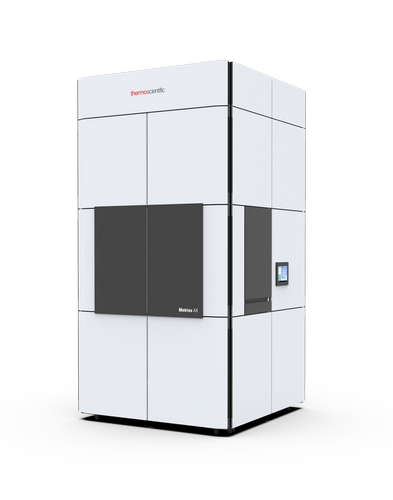
Advanced logic and memory manufacturing processes are becoming more reliant on fast turnaround of precise structural and analytical data to be able to quickly calibrate tool sets, diagnose yield excursions, and optimize process yields. At technology nodes below 28nm, especially in cases where 3D and advanced device designs are being implemented, conventional SEM or optical-based analysis and inspection tools run into challenges that limit their ability to provide robust and reliable data. The Thermo Scientific Metrios AX transmission electron microscope (TEM) is the first TEM dedicated to providing the fast, precise characterization and reference metrology that semiconductor manufacturers need to develop and control their wafer fabrication processes in order to accelerate profitable yield.
High-volume TEM data, accurate and repeatable
The Metrios AX TEM automates the basic TEM operation and measurement procedures, minimizing the requirements for specialized operator training. Its advanced automated metrology routines deliver significantly greater precision than manual methods. The Metrios AX TEM is designed to provide improved throughput and lower cost-per-sample than other TEMs.
Consistent, repeatable, precise
Designed from the ground-up to deliver repeatable TEM and STEM-based imaging, analytics and gauge capable metrology.
Metrology accuracy
Less than 0.75% combined error in distortion and magnification calibration for both TEM and STEM.
Automated EDS and hybrid metrology
Acquire and quantify EDS data with automation. Use elemental contrast on key critical dimensions to extend STEM.
Workflow connectivity
Critical process data is tracked through sample prep, plucking, and imaging. Metrology can be applied offline to maximize tool acquisition time. All imaging and metrology data is consolidated in a web-based image viewer.
Semiconductor Advanced Packaging
Performance, power efficiency, area, and cost are driving packaging innovations. Learn how workflows provide fast, precise, and accurate time-to-data.
Semiconductor research and development
The increasing complexity of semiconductor device structures, along with the shrinking of structural dimensions, means that designing next-generation devices is more challenging and time-consuming than ever before. This, coupled with the fact that the number of technology and design options available is increasing, means a lower probability that any particular design will be commercially successful. As a result, device manufacturers need reliable tools for pathfinding that reduce the number of viable options available and help them implement solutions faster.
Semiconductor metrology
Thermo Fisher Scientific offers a suite of next-generation products with advanced analytical capabilities for semiconductor metrology and inspection. These solutions are designed to help increase productivity in semiconductor fabrication labs by improving quality control and yield in the manufacture of logic, 3D NAND, DRAM, analog, power and display devices.
Semiconductor Failure Analysis
Advanced analytical tools are essential for the detection of any electrical defects that can negatively influence yield, reliability, or performance. With the right equipment, the time and cost associated with electrical fault isolation can be reduced by quickly extracting comprehensive defect data from the sample.
Semiconductor materials characterization
Advanced characterization of these devices can help you deliver on necessary performance, predict and control structural, physical, and chemical properties, as well as correlate your characterization data to parametric test results.
TEM Imaging and Analysis
Thermo Scientific transmission electron microscopes offer high-resolution imaging and analysis of semiconductor devices, enabling manufacturers to calibrate toolsets, diagnose failure mechanisms, and optimize overall process yields.
TEM Metrology
Advanced and automated TEM metrology routines deliver significantly greater precision than manual methods. This allows users to generate large amounts of statistically relevant data, with sub-angstrom-level specificity, that is free of operator bias.








 VI
VI