


")


Increased productivity and data integrity
Higher sample throughput is enabled by the newly redesigned Smart Stage and the new Ultra-X EDS detection system. These features provide an approximate 15% TEM metrology performance increase and 2x faster EDS elemental analysis. The Smart Stage supports fully automated sample loading and precise navigation to the region of interest (ROI). The new constant power lenses enable high-tension switching in less than 20 minutes, increasing tool availability.
Fast elemental analysis
The Metrios 6 (S)TEM with the Ultra-X EDS detector brings a new level of EDS detection to high-throughput solutions. The advanced Ultra-X EDS detector provides a 4.45 srad solid angle, delivering at least 2x greater data collection efficiency than the previous generation of detectors. This enables collection of data in less time while preserving the integrity of beam-sensitive samples. In addition to these capabilities, Ultra-X unlocks new EDS analysis opportunities with the cleanest EDS spectra, (<1% spurious peaks).
Recipe-free automation for (S)TEM metrology
Recipe-free, full automation utilizes machine-learning algorithms to substantially reduce automation set-up time for each new process or sample type to provide ease-of-use and scalability. Application-specific Smart Automation supports a variety of semiconductor device types, such as gate-all-around (GAA), DRAM, and 3D NAND. The new web-based segmenter and object detection algorithm provide 50x faster model training on device structures. Additionally, Smart Automation is extensible to meet future advanced semiconductor R&D and manufacturing requirements.
Yield Ramp and Metrology
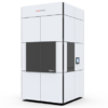
Improving semiconductor yield and accelerating production ramp can be challenging. The increasing 3D complexity of semiconductor devices is generating unprecedented demand for high-quality TEM metrology data. The Metrios 6 (S)TEM features state-of-the-art hardware and machine-learning-based automation software for reference metrology and process monitoring. This solution is designed to help semiconductor labs increase sample throughput and high-volume data acquisition to increase productivity and accelerate time-to-yield.
Physical and Chemical Characterization
Developing modern semiconductor devices requires physical, structural, and elemental characterization on atomic-scale defects with special consideration for electron-beam-sensitive materials. The Metrios 6 (S)TEM supports flexible imaging and characterization workflows for accurate root cause analysis and faster process development. Working on beam-sensitive materials depends on enhanced data collection efficiency and minimum electron-beam exposure to preserve data integrity. The Metrios 6 (S)TEM features the Ultra-X EDS detection system and fast high-tension switching for fast physical and elemental characterization of semiconductor devices.
Memory Device Metrology and Analysis
Manufacturing advanced memory devices, such as 3D NAND and DRAM, requires high-volume, precision TEM metrology on small, critical dimensions hidden in high-aspect-ratio structures. With fully automated workflows, the Metrios 6 (S)TEM delivers high-productivity, high-quality reference metrology and defect analysis for advanced memory device structures.


 VI
VI