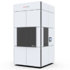
Talos F200C Transmission Electron Microscope
The Thermo Scientific Talos F200C TEM is a 20-200 kV thermionic (scanning) transmission electron microscope uniquely designed for performance and productivity across a wide range of samples and applications, such as 2D and 3D imaging of cells, organelles, asbestos, polymers, and soft materials, both at ambient and cryogenic temperatures.
It elevates the imaging quality of beam-sensitive materials with its optional, motorized, retractable cryo-box and low-dose technique. Additionally, a side-entry retractable energy dispersive spectroscopy (EDS) detector can be added to the configuration to enable chemical analysis. The large C-Twin pole piece gap, which provides high application flexibility, combined with a reproducibly performing electron column, opens new opportunities for high-resolution 3D characterization, in situ dynamic observations, and diffraction applications, with a special emphasis on high-contrast imaging and cryo-TEM. The Talos F200C TEM is equipped with the fast 4k × 4k Thermo Scientific Ceta 16M Camera, which provides a large field-of-view and fast imaging, with high sensitivity, on a 64-bit platform.
Thermo Scientific Maps Software enables intuitive image-based navigation over a whole sample and easy correlation of results across imaging platforms. In order to retrieve large-area imaging at high-resolution Maps Software automatically acquires and stitches images to document the entire area of interest with exceptional quality. Maps Software can be used across tools and within the tool. It supports image import, overlay and alignment from other microscopes, such as SEM and light microscopy. This enables digital zoom from correlated low-magnification TEM and/or SEM to high-resolution TEM (HRTEM), which provides valuable contextual information.
Superior images
High-contrast, high-quality TEM and STEM imaging with simultaneous, multiple signal detection with up to four-channel integrated STEM detectors.
Auto-alignments
All daily TEM tunings, such as focus, eucentric height, center beam shift, center condenser aperture, and rotation center are automated.
Improved productivity and reproducibility
Ultra-stable column and remote operation with SmartCam and constant power objective lenses for quick mode and HT switches. Fast, easy switching for multi-user environments.
Chemical composition data
Flexible EDS analysis reveals chemical information.
Space for more
Large analytical pole piece gap, 180° stage tilt range, and large z-range allow you to add tomography holders, in situ sample holders, and more.
Ceta CMOS Camera
The large field-of-view of the 4k × 4K Ceta CMOS Camera enables live digital zooming with high sensitivity and high speed over the entire high-tension range.
Process control using electron microscopy
Modern industry demands high throughput with superior quality, a balance that is maintained through robust process control. SEM and TEM tools with dedicated automation software provide rapid, multi-scale information for process monitoring and improvement.
Quality control and failure analysis
Quality control and assurance are essential in modern industry. We offer a range of EM and spectroscopy tools for multi-scale and multi-modal analysis of defects, allowing you to make reliable and informed decisions for process control and improvement.
Fundamental Materials Research
Novel materials are investigated at increasingly smaller scales for maximum control of their physical and chemical properties. Electron microscopy provides researchers with key insight into a wide variety of material characteristics at the micro- to nano-scale
Energy Dispersive Spectroscopy
Energy dispersive spectroscopy (EDS) collects detailed elemental information along with electron microscopy images, providing critical compositional context for EM observations. With EDS, chemical composition can be determined from quick, holistic surface scans down to individual atoms.
3D EDS Tomography
Modern materials research is increasingly reliant on nanoscale analysis in three dimensions. 3D characterization, including compositional data for full chemical and structural context, is possible with 3D EM and energy dispersive X-ray spectroscopy.
EDS Elemental Analysis
Thermo Scientific Phenom Elemental Mapping Software provides fast and reliable information on the distribution of chemical elements within a sample.
Atomic-Scale EDS
Atomic-resolution EDS provides unparalleled chemical context for materials analysis by differentiating the elemental identity of individual atoms. When combined with high-resolution TEM, it is possible to observe the precise organization of atoms in a sample.
Electron Energy Loss Spectroscopy (EELS)
Materials science research benefits from high-resolution EELS for a wide range of analytical applications. This includes high-throughput, high signal-to-noise-ratio elemental mapping, as well as probing of oxidation states and surface phonons.
In Situ experimentation
Direct, real-time observation of microstructural changes with electron microscopy is necessary to understand the underlying principles of dynamic processes such as recrystallization, grain growth, and phase transformation during heating, cooling, and wetting.
Particle analysis
Particle analysis plays a vital role in nanomaterials research and quality control. The nanometer-scale resolution and superior imaging of electron microscopy can be combined with specialized software for rapid characterization of powders and particles.
Multi-scale analysis
Novel materials must be analyzed at ever higher resolution while retaining the larger context of the sample. Multi-scale analysis allows for the correlation of various imaging tools and modalities such as X-ray microCT, DualBeam, Laser PFIB, SEM and TEM.
Automated Particle Workflow
The Automated NanoParticle Workflow (APW) is a transmission electron microscope workflow for nanoparticle analysis, offering large area, high resolution imaging and data acquisition at the nanoscale, with on-the-fly processing.


")


 VI
VI