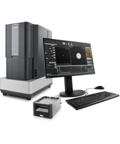
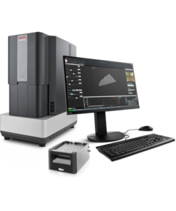
Verios 5 XHR Scanning Electron Microscope
The Verios 5 XHR SEM offers subnanometer resolution over the full 1 keV to 30 keV energy range with excellent materials contrast. Unprecedented levels of automation and ease-of-use make this performance accessible to users of any experience level.
Scanning electron microscopy characterization
- High resolution nanomaterial imaging with the UC+ monochromated electron source for sub-nanometer performance from 1-30 kV.
- High contrast on sensitive materials with excellent performance down to 20 eV landing energy and high-sensitivity in-column and below-the-lens detectors and signal filtering for low-dose operation and optimal contrast selection.
- Greatly reduced time to nanoscale information for users with any experience level using the Elstar electron column featuring SmartAlign and FLASH technologies.
- Consistent measurement results with ConstantPower lenses, electrostatic scanning and a choice of two piezoelectric stages.
- Flexibility for accessories with a large chamber.
- Unattended SEM operation with Thermo Scientific AutoScript 4 Software, an optional Python-based application programming interface.
SmartAlign technology
SmartAlign technology eliminates the need for any user alignments of the electron column, which not only minimizes maintenance, but also increases your productivity.
Innovative electron optics
Including Thermo Scientific’s patented UC+ gun (monochromator), ConstantPower lenses and electrostatic scanning for accurate and stable imaging.
Sub-nanometer resolution
Elstar Schottky monochromated (UC+) FESEM technology and performance with sub-nanometer resolution from 1 to 30 keV.
Consistent measurement results
The Verios is ideally suited to lab-based metrology applications, with the ability to calibrate to a NIST certified standard at high magnification.
Low dose operation and optimal contrast selection
Advanced suite of high-sensitivity, in-column & below-the-lens detectors and signal filtering for low dose operation and optimal contrast selection.
Easy access to beam landing energies
As low as 20 eV with very high resolution for true surface characterization.
Unattended SEM operation
With AutoScript 4 Software, an optional Python-based application programming interface (API).
Large chamber
With a choice of two precise and stable piezo-driven stages.
Fundamental Materials Research
Novel materials are investigated at increasingly smaller scales for maximum control of their physical and chemical properties. Electron microscopy provides researchers with key insight into a wide variety of material characteristics at the micro- to nano-scale.
Semiconductor research and development
The increasing complexity of semiconductor device structures, along with the shrinking of structural dimensions, means that designing next-generation devices is more challenging and time-consuming than ever before. This, coupled with the fact that the number of technology and design options available is increasing, means a lower probability that any particular design will be commercially successful. As a result, device manufacturers need reliable tools for pathfinding that reduce the number of viable options available and help them implement solutions faster.
Semiconductor metrology
Thermo Fisher Scientific offers a suite of next-generation products with advanced analytical capabilities for semiconductor metrology and inspection. These solutions are designed to help increase productivity in semiconductor fabrication labs by improving quality control and yield in the manufacture of logic, 3D NAND, DRAM, analog, power and display devices.
Semiconductor Failure Analysis
Advanced analytical tools are essential for the detection of any electrical defects that can negatively influence yield, reliability, or performance. With the right equipment, the time and cost associated with electrical fault isolation can be reduced by quickly extracting comprehensive defect data from the sample.
Semiconductor materials characterization
Advanced characterization of these devices can help you deliver on necessary performance, predict and control structural, physical, and chemical properties, as well as correlate your characterization data to parametric test results.
Energy dispersive spectroscopy (EDS) collects detailed elemental information along with electron microscopy images, providing critical compositional context for EM observations. With EDS, chemical composition can be determined from quick, holistic surface scans down to individual atoms.
Studying materials in real-world conditions often involves working at high temperatures. The behavior of materials as they recrystallize, melt, deform, or react in the presence of heat can be studied in situ with scanning electron microscopy or DualBeam tools.
Novel materials must be analyzed at ever higher resolution while retaining the larger context of the sample. Multi-scale analysis allows for the correlation of various imaging tools and modalities such as X-ray microCT, DualBeam, Laser PFIB, SEM and TEM.
Cathodoluminescence (CL) describes the emission of light from a material when it is excited by an electron beam. This signal, captured by a specialized CL detector, carries information on the sample’s composition, crystal defects, or photonic properties.


 VI
VI