Additive manufacturing analysis
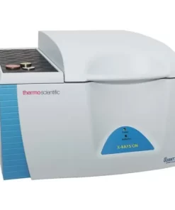
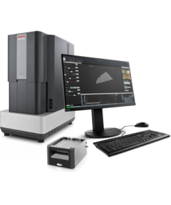
The Thermo Scientific Phenom ParticleX Desktop Scanning Electron Microscope (SEM) is a multi-purpose desktop SEM designed for additive manufacturing, delivering purity at the microscale.
It is equipped with a chamber large enough to analyze samples up to 100 mm x 100 mm. The proprietary venting and loading mechanism ensures the fastest vent/load cycle in the world, providing the highest throughput.
With the Phenom ParticleX AM Desktop SEM, you can take in-house control of your data:
- Monitor critical characteristics of metal powders
- Enhance your powder-bed and powder-fed additive manufacturing processes
- Identify particle size distributions, individual particle morphology, and foreign particles
SEM particle analysis
The Phenom ParticleX AM Desktop SEM features a chamber with an accurate and fast motorized stage that allows analysis of samples of up to 100 mm x 100 mm. Even with this larger sample size, the proprietary loading shuttle keeps the vent/load cycle to an industry-leading loading time of 60 seconds or less, ultimately delivering faster throughput than other SEM systems.
Additive manufacturing testing
The Phenom ParticleX AM Desktop SEM measures various size and shape parameters, such as minimum and maximum diameter, perimeter, aspect ratio, roughness, and feret diameter. All of these can be displayed with 10%, 50%, or 90% values (i.e., d10, d50, d90).
SEM elemental mapping
The elemental mapping and line scan functionality lets you start working with a single click. The line scan functionality shows the quantified element distribution in a line plot. This is especially useful for analyzing edges, coatings, and cross sections of coatings, paints, and other samples with multiple layers.
Secondary electron detector
An optional secondary electron detector (SED) can be added to the Phenom ParticleX AM Desktop SEM. The SED collects low-energy electrons from the top surface layer of the sample, making it ideally suited to revealing detailed sample surface information. The SED can be of great use for studying microstructures, fibers, and particles or other applications where topography and morphology are important.
Process control using electron microscopy
Modern industry demands high throughput with superior quality, a balance that is maintained through robust process control. SEM and TEM tools with dedicated automation software provide rapid, multi-scale information for process monitoring and improvement.
Quality control and failure analysis
Quality control and assurance are essential in modern industry. We offer a range of EM and spectroscopy tools for multi-scale and multi-modal analysis of defects, allowing you to make reliable and informed decisions for process control and improvement.
Fundamental Materials Research
Novel materials are investigated at increasingly smaller scales for maximum control of their physical and chemical properties. Electron microscopy provides researchers with key insight into a wide variety of material characteristics at the micro- to nano-scale.
Technical Cleanliness
More than ever, modern manufacturing necessitates reliable, quality components. With scanning electron microscopy, parts cleanliness analysis can be brought inhouse, providing you with a broad range of analytical data and shortening your production cycle.
EDS Elemental Analysis
Thermo Scientific Phenom Elemental Mapping Software provides fast and reliable information on the distribution of chemical elements within a sample.
3D EDS Tomography
Modern materials research is increasingly reliant on nanoscale analysis in three dimensions. 3D characterization, including compositional data for full chemical and structural context, is possible with 3D EM and energy dispersive X-ray spectroscopy.
Atomic-Scale Elemental Mapping with EDS
Atomic-resolution EDS provides unparalleled chemical context for materials analysis by differentiating the elemental identity of individual atoms. When combined with high-resolution TEM, it is possible to observe the precise organization of atoms in a sample.
Particle analysis
Particle analysis plays a vital role in nanomaterials research and quality control. The nanometer-scale resolution and superior imaging of electron microscopy can be combined with specialized software for rapid characterization of powders and particles.


 VI
VI