Materials characterization
Advanced materials characterization labs require access to the latest techniques and will push analytical tools, including SEMs, to the extremes of their capabilities. Most of these labs are multi-user facilities that accommodate users with varying degrees of experience. Time on the microscope is precious, and excessive time spent on maintenance, alignments, training, or image optimization needs to be avoided.
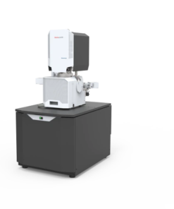
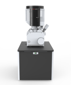
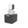
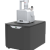
Apreo 2 Scanning Electron Microscope
The new Thermo Scientific Apreo 2 SEM expands access to high-performance imaging and analytics to all levels of microscopy expertise. With Thermo Scientific ChemiSEM Technology, a unique live elemental imaging capability, compositional information is always available, through the most intuitive interface. Eliminating all the hassle associated with typical EDS implementations, ChemiSEM Technology offers unprecedented time to result and ease of use.
The Apreo 2 SEM poses much smaller demands on users and lab managers with Thermo Scientific SmartAlign Technology, an optics system that aligns itself. Furthermore, the Apreo 2 SEM automates the image fine-tuning process with Thermo Scientific FLASH technology. FLASH Technology executes any necessary corrections to lens centering, the stigmators, and final focus of the image. The combination of these technologies means that users new to electron microscopy can access the high-end performance of the Apreo 2 SEM. Additionally, the Apreo 2 SEM is the only SEM with a 1-nanometer resolution at 10 mm analytical working distance. No longer does long working distance mean poor imaging. With the Apreo 2 SEM, anyone will be able to confidently get great results.
High performance, resolution, and contrast
The combination of advanced optics, detection and automation in Apreo 2 makes obtaining high resolution imaging possible even for users new to SEM.
Wide range of sample types
Apreo 2 was designed for maximum flexibility. High quality, high resolution imaging is possible regardless of target samples properties. Insulators, beam sensitive or magnetic materials can all be imaged with ease thanks to Apreo 2’s unique optics, detection and beam control options.
Live quantitative EDS with ChemiSEM
Elemental information at your fingertips with ChemiSEM, which provides live quantitative elemental mapping for unprecedented time to result and ease of use.
Quick and easy sample loading
Easy access to the stage, a convenient multi-sample holder, and a fast pump down ensures no time is wasted loading samples. An automated routine to insert and remove a pressure limiting aperture (PLA) allows for a seamless switch between high and low vacuum without opening the chamber.
Advanced automation
From optics, to image acquisition, Apreo 2 provides a range of automated features to make imaging time as effective and efficient as possible. Flash Technology automates image fine tuning The unique Undo function permits efficient exploration of imaging conditions Thermo Scientific Maps software automates large area acquisition with up to 4 different simultaneous signals
Performance at long working distance
Apreo 2 is the only SEM that offers high-resolution performance (1nm) and excellent image quality at analytical working distance (10mm). Sample morphology, topography and surface information can all be simultaneously explored while being at a safe distance from the pole piece. Thanks to its high-speed and high-sensitivity in-lens backscattered detector, BSE are still detected even at extremely low beam currents (as low as few pA).
Process control using electron microscopy
Modern industry demands high throughput with superior quality, a balance that is maintained through robust process control. SEM and TEM tools with dedicated automation software provide rapid, multi-scale information for process monitoring and improvement.
Quality control and failure analysis
Quality control and assurance are essential in modern industry. We offer a range of EM and spectroscopy tools for multi-scale and multi-modal analysis of defects, allowing you to make reliable and informed decisions for process control and improvement.
Fundamental Materials Research
Novel materials are investigated at increasingly smaller scales for maximum control of their physical and chemical properties. Electron microscopy provides researchers with key insight into a wide variety of material characteristics at the micro- to nano-scale.
Semiconductor research and development
The increasing complexity of semiconductor device structures, along with the shrinking of structural dimensions, means that designing next-generation devices is more challenging and time-consuming than ever before. This, coupled with the fact that the number of technology and design options available is increasing, means a lower probability that any particular design will be commercially successful. As a result, device manufacturers need reliable tools for pathfinding that reduce the number of viable options available and help them implement solutions faster.
Semiconductor metrology
Thermo Fisher Scientific offers a suite of next-generation products with advanced analytical capabilities for semiconductor metrology and inspection. These solutions are designed to help increase productivity in semiconductor fabrication labs by improving quality control and yield in the manufacture of logic, 3D NAND, DRAM, analog, power and display devices.
Semiconductor Failure Analysis
Advanced analytical tools are essential for the detection of any electrical defects that can negatively influence yield, reliability, or performance. With the right equipment, the time and cost associated with electrical fault isolation can be reduced by quickly extracting comprehensive defect data from the sample.
Semiconductor materials characterization
Advanced characterization of these devices can help you deliver on necessary performance, predict and control structural, physical, and chemical properties, as well as correlate your characterization data to parametric test results.
Energy dispersive X-ray spectroscopy for materials characterization.
Energy dispersive spectroscopy (EDS) collects detailed elemental information along with electron microscopy images, providing critical compositional context for EM observations. With EDS, chemical composition can be determined from quick, holistic surface scans down to individual atoms.
Studying materials in real-world conditions often involves working at high temperatures. The behavior of materials as they recrystallize, melt, deform, or react in the presence of heat can be studied in situ with scanning electron microscopy or DualBeam tools.
Novel materials must be analyzed at ever higher resolution while retaining the larger context of the sample. Multi-scale analysis allows for the correlation of various imaging tools and modalities such as X-ray microCT, DualBeam, Laser PFIB, SEM and TEM.


 VI
VI