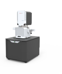
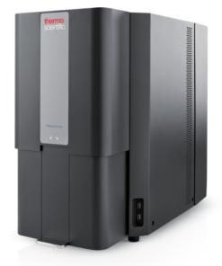
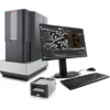
Phenom Desktop SEM with energy-dispersive X-ray diffraction
The sixth-generation of Thermo Scientific Phenom ProX G6 Desktop SEM fills the gap between light microscopy and floor-model SEM analysis, thus expanding the capabilities of research facilities. It offers fast, high-resolution imaging in addition to an integrated energy-dispersive X-ray diffraction (EDS) detector for robust, easy-to-use, rapid elemental analysis.
Fast and easy to use
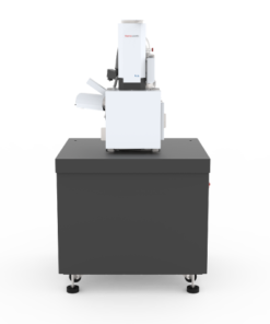
The Phenom Pro Desktop SEM can be used to relieve the burden of routine analysis for common samples from floor-model SEM instruments. Instrument configuration and the sample loading mechanism ensure quick imaging with minimal time spent tuning between experiments.
Long-lifetime CeB6 source
Facility users of any experience level can quickly begin producing high-quality results with the Phenom Pro Desktop SEM. Its long-lifetime CeB6 source offers high brightness while requiring low maintenance.
Robust and small form factor
It’s high stability and small form factor allow the instrument to be used in practically any lab environment; more simply put, it does not require specialized infrastructure or expert oversight.
Process control using electron microscopy
Modern industry demands high throughput with superior quality, a balance that is maintained through robust process control. SEM and TEM tools with dedicated automation software provide rapid, multi-scale information for process monitoring and improvement.
Quality control and failure analysis
Quality control and assurance are essential in modern industry. We offer a range of EM and spectroscopy tools for multi-scale and multi-modal analysis of defects, allowing you to make reliable and informed decisions for process control and improvement.
Fundamental Materials Research
Novel materials are investigated at increasingly smaller scales for maximum control of their physical and chemical properties. Electron microscopy provides researchers with key insight into a wide variety of material characteristics at the micro- to nano-scale.
Semiconductor research and development
The increasing complexity of semiconductor device structures, along with the shrinking of structural dimensions, means that designing next-generation devices is more challenging and time-consuming than ever before. This, coupled with the fact that the number of technology and design options available is increasing, means a lower probability that any particular design will be commercially successful. As a result, device manufacturers need reliable tools for pathfinding that reduce the number of viable options available and help them implement solutions faster.
Semiconductor metrology
Thermo Fisher Scientific offers a suite of next-generation products with advanced analytical capabilities for semiconductor metrology and inspection. These solutions are designed to help increase productivity in semiconductor fabrication labs by improving quality control and yield in the manufacture of logic, 3D NAND, DRAM, analog, power and display devices.
Semiconductor Failure Analysis
Advanced analytical tools are essential for the detection of any electrical defects that can negatively influence yield, reliability, or performance. With the right equipment, the time and cost associated with electrical fault isolation can be reduced by quickly extracting comprehensive defect data from the sample.
Semiconductor materials characterization
Advanced characterization of these devices can help you deliver on necessary performance, predict and control structural, physical, and chemical properties, as well as correlate your characterization data to parametric test results.
EDS Elemental Analysis
Thermo Scientific Phenom Elemental Mapping Software provides fast and reliable information on the distribution of chemical elements within a sample.
3D EDS Tomography
Modern materials research is increasingly reliant on nanoscale analysis in three dimensions. 3D characterization, including compositional data for full chemical and structural context, is possible with 3D EM and energy dispersive X-ray spectroscopy.
Atomic-Scale Elemental Mapping with EDS
Atomic-resolution EDS provides unparalleled chemical context for materials analysis by differentiating the elemental identity of individual atoms. When combined with high-resolution TEM, it is possible to observe the precise organization of atoms in a sample.
Imaging Hot Samples
Studying materials in real-world conditions often involves working at high temperatures. The behavior of materials as they recrystallize, melt, deform, or react in the presence of heat can be studied in situ with scanning electron microscopy or DualBeam tools.
In Situ experimentation
Direct, real-time observation of microstructural changes with electron microscopy is necessary to understand the underlying principles of dynamic processes such as recrystallization, grain growth, and phase transformation during heating, cooling, and wetting.
Multi-scale analysis
Novel materials must be analyzed at ever higher resolution while retaining the larger context of the sample. Multi-scale analysis allows for the correlation of various imaging tools and modalities such as X-ray microCT, DualBeam, Laser PFIB, SEM and TEM.
SEM Metrology
Scanning electron microscopy provides accurate and reliable metrology data at nanometer scales. Automated ultra-high-resolution SEM metrology enables faster time-to-yield and time-to-market for memory, logic, and data storage applications.
Semiconductor Analysis and Imaging
Thermo Fisher Scientific offers scanning electron microscopes for every function of a semiconductor lab, from general imaging tasks to advanced failure analysis techniques requiring precise voltage-contrast measurements.


 VI
VI