SEM imaging and EDS elemental analysis
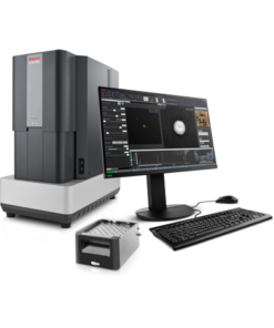
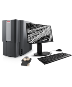
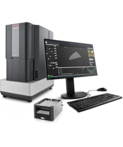
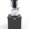
Even though scanning electron microscopy (SEM) has made tremendous advances, it can be considered by new users to be a complicated technique. Sample preparation, alignments, cost of ownership, and difficulties with analytical techniques prevent widespread adoption. We set out to resolve these challenges in order to make a truly accessible SEM without compromising on flexibility. Our goal was to make microscopy an easy and enjoyable experience in which you should not have to fight the microscope to obtain quality data. The result is the Thermo Scientific Axia ChemiSEM Scanning Electron Microscope, a system in which obtaining SEM-EDS data is no longer a chore. EDS is no longer just an afterthought—chemical data and imaging have now become one.
SEM EDS analysis
The Axia ChemiSEM is unlike traditional SEMs in that it always collects EDS data in the background. It uses unique algorithms to process the SEM and EDS signals simultaneously, allowing it to display the morphology and quantitative elemental make up of a sample together, in real time. It constantly processes EDS data in the background, giving you live updates on elemental data, as it is acquired. Elements found in your sample can be toggled on and off, allowing you to isolate areas of interest.
The Axia ChemiSEM features a superior user experience enhanced by automation, such as SmartAlign technology for alignment-free operation, newly developed automatic functions, and live quantitative EDS mapping. This always-on processing make analysis twice as fast, compared to traditional methods. The Axia ChemiSEM Scanning Electron Microscope puts SEM/EDS analysis within reach of a wider scientific audience, speeds up your workflow, and saves time on training.
Live quantitative elemental mapping
Update your Analytical workflow with fully integrated, cutting-edge Thermo Scientific ChemiSEM technology that provides characterization in half the time.
Easy to get started
Integrated User Guidance, live real-time compositional imaging, and alignment-free operation combine on this instrument to allow you to stay focused on data collection.
Flexible sample loading
The flexible stage accommodates samples up to 10 kg with x-y movement, and the door opens fully for easy loading of large, awkward samples – while retaining a very fast pump down time.
Excellent imaging performance
Easily handle a wide range of applications, including insulating samples with Low Vac operation and advanced beam scanning to ensure high-fidelity imaging
Diverse application software
Handle advanced applications with advanced system automation option, such as Thermo Scientific Maps™ Software, and customize workflow development with Thermo Scientific AutoScript™ Software.
Easy maintenance
Source exchange is easy and can be completed by any user, while the straightforward design translates to high uptime and rapid service when attention is needed.
Process control using electron microscopy
Modern industry demands high throughput with superior quality, a balance that is maintained through robust process control. SEM and TEM tools with dedicated automation software provide rapid, multi-scale information for process monitoring and improvement.
Quality control and failure analysis
Quality control and assurance are essential in modern industry. We offer a range of EM and spectroscopy tools for multi-scale and multi-modal analysis of defects, allowing you to make reliable and informed decisions for process control and improvement.
Fundamental Materials Research
Novel materials are investigated at increasingly smaller scales for maximum control of their physical and chemical properties. Electron microscopy provides researchers with key insight into a wide variety of material characteristics at the micro- to nano-scale.
Energy dispersive X-ray spectroscopy for materials characterization.
Studying materials in real-world conditions often involves working at high temperatures. The behavior of materials as they recrystallize, melt, deform, or react in the presence of heat can be studied in situ with scanning electron microscopy or DualBeam tools.
Particle analysis plays a vital role in nanomaterials research and quality control. The nanometer-scale resolution and superior imaging of electron microscopy can be combined with specialized software for rapid characterization of powders and particles.








 VI
VI