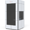
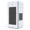
Spectra 300 Transmission Electron Microscope
For scientists to advance their understanding of complex samples and develop innovative materials, they must have access to robust, precise instrumentation capable of correlating form and function, as well as resolving space, time and frequency.
Thermo Fisher Scientific introduces the Thermo Scientific Spectra 300 (S)TEM – the highest resolution, aberration corrected, scanning transmission electron microscope for all materials science applications.
Spectra 300 Transmission Electron Microscope advantages
All Spectra 300 (S)TEM’s are delivered on new platforms designed to offer an unprecedented level of mechanical stability and highest imaging quality though passive and (optional) active vibration isolation.
The system is housed in a fully redesigned enclosure with a built-in on-screen display for convenient specimen loading and removal. For the first time, full modularity and upgradeability can be offered between uncorrected and single-corrected configurations with variable heights, allowing maximum flexibility for different room configurations.
High energy resolution sources available on the Spectra 300 (S)TEM
The Spectra 300 (S)TEM can be optionally equipped with either a high-energy-resolution extreme field emission gun (X-FEG)/Mono or an ultra-high-energy resolution X-FEG/UltiMono. The monochromators of both sources are automatically excited and tuned with single-click operation to achieve the highest energy resolution possible on each configuration by using OptiMono or OptiMono+ respectively (see video below).
Also configurable with the ultra-high brightness X-CFEG source
The Spectra 300 (S)TEM can optionally be powered by a new cold field emission gun (X-CFEG). The X-CFEG has extremely high brightness (>>1.0 x 10⁸ A/m2/Sr/V*), low energy spread (<0.4 eV), and can operate from 30 – 300 kV. This provides simultaneously high-resolution STEM imaging with high probe currents for high throughput, fast acquisition STEM analytics in parallel with high-energy resolution. With the powerful combination of X-CFEG and the S-CORR probe aberration corrector, sub-Angstrom (<0.8 Å) STEM-imaging resolution with over 1000 pA of probe current can be routinely achieved.
Providing the highest resolution STEM imaging performance
The combination of enhanced mechanical stability, the latest 5th-order probe aberration correction and the high-resolution (S-TWIN) wide-gap pole piece results in an instrument with the highest commercially-available STEM resolution specifications.
Unprecedented sensitivity with the Panther STEM detection system
STEM imaging on the Spectra (S)TEM has been reimagined with the Panther STEM detection system, which includes a new data acquisition architecture and two new, solid state, eight-segment ring and disk STEM detectors (16 segments in total). The new detector geometry offers access to advanced STEM imaging capability combined with the sensitivity to measure single electrons.
Advanced STEM imaging capabilities
The Spectra 300 (S)TEM can be configured with an electron microscope pixel array detector (EMPAD) or a Thermo Scientific Ceta Camera with speed enhancement to collect 4D STEM data sets.
Spectroscopic flexibility with the Spectra 300 (S)TEM
From high-throughput, high signal-to-noise ratio elemental mapping in EDS and EELS to oxidation state and surface phonon probing with ultra-high-resolution EELS, the Spectra 300 (S)TEM offers the spectroscopic flexibility to accommodate the widest range of analytical requirements.
In situ capabilities of the Spectra 300 (S)TEM
The Spectra 300 (S)TEM accepts a wide range of holders for in situ experiments with its all-in-one S-TWIN wide-gap pole piece. The Thermo Scientific NanoEx holder family can be seamlessly integrated with the microscope, enabling MEMS device-based heating for atomic imaging at elevated temperatures.
Process control using electron microscopy
Modern industry demands high throughput with superior quality, a balance that is maintained through robust process control. SEM and TEM tools with dedicated automation software provide rapid, multi-scale information for process monitoring and improvement.
Quality control and failure analysis
Quality control and assurance are essential in modern industry. We offer a range of EM and spectroscopy tools for multi-scale and multi-modal analysis of defects, allowing you to make reliable and informed decisions for process control and improvement.
Fundamental Materials Research
Novel materials are investigated at increasingly smaller scales for maximum control of their physical and chemical properties. Electron microscopy provides researchers with key insight into a wide variety of material characteristics at the micro- to nano-scale
Semiconductor research and development
The increasing complexity of semiconductor device structures, along with the shrinking of structural dimensions, means that designing next-generation devices is more challenging and time-consuming than ever before. This, coupled with the fact that the number of technology and design options available is increasing, means a lower probability that any particular design will be commercially successful. As a result, device manufacturers need reliable tools for pathfinding that reduce the number of viable options available and help them implement solutions faster.
Semiconductor Failure Analysis
Advanced analytical tools are essential for the detection of any electrical defects that can negatively influence yield, reliability, or performance. With the right equipment, the time and cost associated with electrical fault isolation can be reduced by quickly extracting comprehensive defect data from the sample.
Semiconductor display technology
Display technologies are evolving to improve display quality and light conversion efficiency. Learn how metrology, failure analysis, and characterization solutions provide insights.
Energy Dispersive Spectroscopy
Energy dispersive spectroscopy (EDS) collects detailed elemental information along with electron microscopy images, providing critical compositional context for EM observations. With EDS, chemical composition can be determined from quick, holistic surface scans down to individual atoms.
3D EDS Tomography
Modern materials research is increasingly reliant on nanoscale analysis in three dimensions. 3D characterization, including
Atomic-Scale EDS
Atomic-resolution EDS provides unparalleled chemical context for materials analysis by differentiating the elemental identity of individual atoms. When combined with high-resolution TEM, it is possible to observe the precise organization of atoms in a sample.
EDS Elemental Analysis
Thermo Scientific Phenom Elemental Mapping Software provides fast and reliable information on the distribution of chemical elements within a sample.
Electron Energy Loss Spectroscopy (EELS)
Materials science research benefits from high-resolution EELS for a wide range of analytical applications. This includes high-throughput, high signal-to-noise-ratio elemental mapping, as well as probing of oxidation states and surface phonons.
In Situ experimentation
Direct, real-time observation of microstructural changes with electron microscopy is necessary to understand the underlying principles of dynamic processes such as recrystallization, grain growth, and phase transformation during heating, cooling, and wetting.
Particle analysis
Particle analysis plays a vital role in nanomaterials research and quality control. The nanometer-scale resolution and superior imaging of electron microscopy can be combined with specialized software for rapid characterization of powders and particles.
Multi-scale analysis
Novel materials must be analyzed at ever higher resolution while retaining the larger context of the sample. Multi-scale analysis allows for the correlation of various imaging tools and modalities such as X-ray microCT, DualBeam, Laser PFIB, SEM and TEM.
TEM Imaging and Analysis
Thermo Scientific transmission electron microscopes offer high-resolution imaging and analysis of semiconductor devices, enabling manufacturers to calibrate toolsets, diagnose failure mechanisms, and optimize overall process yields.
Automated Particle Workflow
The Automated NanoParticle Workflow (APW) is a transmission electron microscope workflow for nanoparticle analysis, offering large area, high resolution imaging and data acquisition at the nanoscale, with on-the-fly processing.


")


 VI
VI