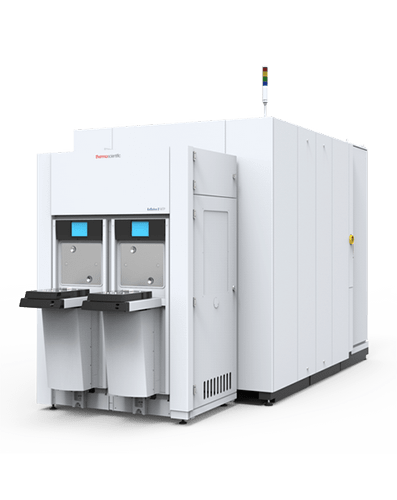
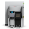
The Thermo Scientific ExSolve wafer TEM prep (WTP) DualBeam (FIB-SEM) dramatically reduces the cost and increases the speed of sample preparation, providing semiconductor and data storage manufacturers with quick and easy access to the data they need to verify and monitor process performance. The ExSolve DualBeam can prepare site-specific TEM lamella, sampling many sites per wafer in a fully-automated process inside the fab, giving semiconductor manufacturers much more information than conventional approaches, while at the same time reducing the capital cost of sample preparation by up to 70 percent.
The ExSolve WTP DualBeam system is an automated, high-throughput sample preparation system that can prepare site-specific, 20 nm thick lamellae on whole wafers up to 300 mm in diameter. It is part of a fast, complete workflow that includes Thermo Scientific TEMLink, and the Thermo Scientific Metrios TEM. The ExSolve DualBeam includes FOUP handling and is designed to be located in the fab near the manufacturing line.
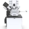
The ExSolve WTP DualBeam workflow addresses the needs of customers that require automated, high-throughput sampling at advanced technology nodes. It complements the capabilities of the Thermo Scientific Helios NanoLab DualBeam 1200AT, which provides more flexible, operator-directed, sample preparation methods, along with additional capabilities such as high-resolution scanning electron microscopy (SEM) imaging and analysis.
Semiconductor research and development
The increasing complexity of semiconductor device structures, along with the shrinking of structural dimensions, means that designing next-generation devices is more challenging and time-consuming than ever before. This, coupled with the fact that the number of technology and design options available is increasing, means a lower probability that any particular design will be commercially successful. As a result, device manufacturers need reliable tools for pathfinding that reduce the number of viable options available and help them implement solutions faster.
Semiconductor metrology
Thermo Fisher Scientific offers a suite of next-generation products with advanced analytical capabilities for semiconductor metrology and inspection. These solutions are designed to help increase productivity in semiconductor fabrication labs by improving quality control and yield in the manufacture of logic, 3D NAND, DRAM, analog, power and display devices.
Semiconductor Failure Analysis
Advanced analytical tools are essential for the detection of any electrical defects that can negatively influence yield, reliability, or performance. With the right equipment, the time and cost associated with electrical fault isolation can be reduced by quickly extracting comprehensive defect data from the sample.
Semiconductor materials characterization
Advanced characterization of these devices can help you deliver on necessary performance, predict and control structural, physical, and chemical properties, as well as correlate your characterization data to parametric test results.
TEM Sample Prep
Thermo Scientific DualBeam systems provide accurate TEM sample preparation for atomic-scale analysis of semiconductor devices. Automation and advanced machine learning technologies produce high-quality samples, at the correct location, and a low cost per sample.
TEM Metrology
Advanced and automated TEM metrology routines deliver significantly greater precision than manual methods. This allows users to generate large amounts of statistically relevant data, with sub-angstrom-level specificity, that is free of operator bias.






 VI
VI