Online Support

GeminiSEM – Field Emission Scanning Electron Microscopes (FE-SEM)

ZEISS GeminiSEM stands for effortless imaging with sub-nanometer resolution. These FE-SEMs (field emission scanning electron microscope) combine excellence in imaging and analytics. Innovations in electron optics and a new chamber design let you benefit from better image quality, usability and flexibility. Take sub-nanometer images below 1 kV without an immersion lens. Discover three unique designs of the ZEISS Gemini electron optics.

  • Ideal for core facilities – ZEISS GeminiSEM 360
  • Enabling efficient analysis – ZEISS GeminiSEM 460
  • New standard for surface imaging – ZEISS GeminiSEM 560

Applications in Materials Science

  • Image and analyze any real-world sample effortlessly, over large areas or at sub-nanometer resolution.
  • Explore examples from nanoscience, engineering and energy materials, or bio-inspired materials, polymers & catalysts.
  • See how GeminiSEM helps you to characterize your specimen comprehensively.

Microscopy Solutions for Industry

  • Failure analysis on mechanical, optical or electronic components
  • Fracture analysis and metallography
  • Surface, microstructure and device characterization
  • Compositional and phase distribution
  • Impurity and inclusion determination

Applications in Electronics & Semiconductor

  • Construction analysis and benchmarking
  • Passive voltage contrast
  • Subsurface analysis
  • Electronic property measurement with probing
  • TEM site selection

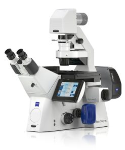
Applications in Life Sciences

  • Characterization of topology
  • Imaging sensitive, non-conductive, outgassing, or low contrast samples
  • Visualizing the ultrastructure of cells, tissues etc. at high resolutions
  • Imaging very large areas such as serial sections or block faces

Your Tool for Sample Flexibility

  • GeminiSEM 360 is the ideal instrument for a core facility, delivering maximum versatility for materials & life science, and industry.
  • The eponymous electron optical design Gemini 1 brings you the benefit of surface sensitive, high resolution images providing excellent resolution at low voltage and great speed at high probe current.
  • Gather high resolution, surface- and compositional information, even on sensitive samples by using Inlens secondary and backscatter electron imaging simultaneously.
  • When aiming to image non-conducting samples under lower vacuum, so-called variable pressure, there is no need to forgo Inlens contrast: NanoVP guarantees maximum versatility enabling Inlens imaging without charging.

Unrivalled User Experience

  • GeminiSEM 360 delivers exceptional user experience: With its wide field of view and new, highly configurable chamber, it’s easy to interrogate even very large samples.
  • Enjoy seamless navigation with contextual image viewing and correlative microscopy via ZEISS ZEN Connect.
  • Gain clear, crisp images easily by using autofunctions e.g. the autofocus and smart detectors.
  • Perform both imaging and analytical workflows efficiently with diametrically opposite EDS ports and a coplanar EDS/EBSD geometry.
  • Maximize system uptime with ZEISS Predictive Service and benefit from scheduled maintenance to take place when you are ready.

Exceptional Capability Extension

  • Upgradability is essential for protecting your investment. That‘s why GeminiSEM 360 is plugged into the software ecosystem of ZEISS ZEN core.
  • Draw on ZEN Connect to combine multimodal and multiscale data, ZEN Intellesis for advanced AI- powered segmentation, and ZEN’s analytical modules for reporting and analysis of segmented data. ZEN data storage lets you manage projects centrally by connecting data from different instruments in your lab.
  • Access workflows and scripts created by other users who can help you solve challenges by being a member of the APEER community.
  • Improve your system as new capabilities are released thanks to a clear upgrade ability path.

Utilize High Resolution and High Current

  • GeminiSEM 460 is made for your most exacting analytical tasks and enables efficient analysis and unattended workflows.
  • Perform high-resolution imaging and analytics rapidly: switch seamlessly from low current-low kV work to high current-high kV work, and back again utilizing the Gemini 2 column.
  • Characterize any specimen comprehensively by using multiple detectors in parallel.
  • For efficient analysis exploit the versatile chamber and choose appropriate analytical detectors.
  • Use the new VP mode and turn up the current to obtain EBSD maps with indexing rates of 4000 patterns/s.
  • Investigate chemical composition and crystal orientation with two diametrically opposite EDS ports and a coplanar EDS/EBSD configuration. Count on high speed, shadow-free mapping.

Customized, Automated Workflows

  • With such powerful analytics at hand workflow automation becomes key. Create and configure automated experiments of your own with the Python scripting API from ZEISS.
  • Modify experiments and customize the outcome to your own requirements.
  • Make the most of STEM tomography: combine automated tilting and rotation with feature tracking. Produce 3D tomograms with nanometer-scale resolution after all aligned images are then sent to a proprietary 3D reconstruction software.
  • When you need to test materials to their engineering limits, ZEISS puts an automated in situ heating and tension experimental lab at your disposal: it lets you observe materials under heat and tension automatically while plotting stress-strain curves on the fly

Your Pathway to Even More Possibilities

  • Expand your analytical capabilities across materials and life sciences with exceptionally high, tunable current density, even at low kV – based on the Gemini 2 design.
  • Take advantage of being able to adapt the system with a wide variety of accessories. The versatile chamber can be configured not only with analytical equipment but also with devices for in situ experiments, cryo-imaging and nanoprobing. storage lets you manage projects centrally by connecting data from different instruments in your lab.
  • This lets you benefit from the ability to accommodate many configurations and upgrades at any point during the lifetime of your instrument.
  • All GeminiSEMs are plugged into the ZEISS ZEN core ecosystem giving you access to ZEN Connect, ZEN Intellesis and ZEN’s analytical modules providing reporting and GxP workflows.

Image Below 1kV Easily

  • Gemini 3 enables magnetic field-free imaging with sub 1 nm resolution below 1 kV – without the need for sample biasing or monochromation. It includes the Nano-twin lens and the new electron optical engine Smart Autopilot.
  • Achieve images of non-conducting matter with a new variable pressure mode and detection system: ensure fast results and preserve features by bringing vacuum-sensitive specimens into the chamber through the new Gentle Airlock in VP mode.
  • Analyze delicate samples with ease by leveraging the new, large chamber with dual EDS ports. Produce fast, shadow-free mapping ensured by an optimum detector solid angle.

Expert Knowledge Integrated

  • Perform easy sample navigation by leveraging the greatly increased system’s field of view.
  • Imaging of challenging samples is now accelerated by the new electron optical engine Smart Autopilot. It lets you save time while making lengthy alignments obsolete: the engine drives the electron optics to provide magnifications from less than 1× up to 500kx, taking care of alignment, calibration and focus along the way. A new patented parallax autofocus is included and a new auto-wobble provides you with clear, crisp images within seconds.
  • Python scripting is able to use these features in automated workflows such as 3D STEM tomography.

Experience Unique Contrast

  • Finding the sweet spot in your working conditions means that you’ve selected exactly the right combination of parameters to achieve the perfect image: the trick is finding it. Gemini technology with its magnetic field-free imaging and the new Gemini 3 column lets you find these sweet spots and discover new information.
  • Magnetic contrast imaging is easy with a magnetic field on the sample of less than 2 mT. Perform energy spectroscopic imaging with the energy-selective Inlens back-scatter detector and electron angular spectroscopic imaging with the annular backscatter detector.
  • Bring all your data together with ZEN Connect to segment and report on your findings.